Sabtu, 23 April 2011

The CW transmitter


The CW transmitter transmits continuous wave modulation with Morse code. With ‘config’ button you can configure transmission speed & frequency. With ‘load’ you can load a transmitted text from a file. Please note, that the CW transmitter automatically converts lowercase letters to uppercase letters. ‘Start/Stop’ starts and stops the transmission. When the characters are transmitted, the red text ‘transmitting’ is shown in the dialog. If the yellow text ‘ready to transmit’ is shown, you should press the green button in the configuration editor to start the transmission. With ‘reset’ you can reset the transmitter. The CW transmitter shows the currently transmitted character as inverted.

Magnitude

With this you can set the magnitude (maximum amplitude) of the transmitted signal. The amplitude value is set as an absolute value. When 16-bit processing is used then maximum magnitude will be 32767. If 8-bit processing is used the maximum is 127.

Carrier frequency

This sets the carrier frequency. Please note, that if the transmission is connected directly to one of SkySweeper’s own decoders, the FFT resolution is limited, which might cause the situation that the decoder doesn’t lock exactly to the same frequency which is sent. This effect has no influence on the performance of the decoder.

Words per minute

This sets the transmission speed.

Sum to RX
With this switch, you can select the input signal of the CW transmission block added to CW transmission generated by the block. This is very useful feature, when you would like to build multicarrier CW transmissions (just put several CW transmitters in chain with this switch set on)

Repeat
With this switch you can set if the text in the transmitter dialog will be repeated when the last character is sent. The repeated block starts from the cursor position.

Character Set Definition
By clicking this button, the CW character set can be changed.in the Character Set Configuration Dialog

CW Keying Parameters
By clicking this button, the CW keying feature can be enabled. CW transmitter can control radio transmitter through serial port. Parameters can be changed in the CW Keying Configuration Dialog.

Macro
The ‘Macro’ button opens or closes the TX macro panel.

Load
The load button opens the transmitter load data control dialog, which is used to read text from file or socket into transmission text window.

Start
The ‘Start’ button starts transmission from the cursor position. If there are text is selected in the transmission window, only selected text is sent. It is not possible to edit transmission window when transmission is on. Transmission can be stopped any time pressing the ‘Stop’ button. If the TX control signal is enabled start and stop button sets the signal on and off.

Reset
The Reset button clears the transmission window and resets the transmitter.
READ MORE - The CW transmitter

modulation should be aimed in voice transmission


modulation should be aimed in voice transmission

The power of a modulated wave is found from the formula:

Pmod=(1+m2/2) x Pcarr

Where Pmod=Power of the modulated wave,

M=degree of modulation,

Pcarr=power in the carrier frequency.

The power in an amplitude modulated wave is divided between the carrier and the two side bands. The carrier power is constant, and so, the side band power is the difference between the carrier power and the total power in the modulated wave. The above formula is to find the power of the modulated wave when carrier is modulated by single sinusoidal tone.

If the carrier power=50 watts

%ge of modulation=100 or 1

degree of modulation=1

Then the power of the modulated wave,

Pmod=(1+m2/2) x 50=3/2 x 50 = 75 watts

Since the carrier power = 50 watts; the two side bands have 25 watts in them, i.e.

25/75 x 100% = 33.3% of the total power with 100% modulation.

In case of 50% modulation with same carrier power we have,

Pmod=(1+0.52/2) x 50 = 2.25/2 x 50 = 56.25 watts

Now the side bands have only 6.25 watts (since 56.25-50 = 6.25)

Since all the intelligence being transmitted is contained in the side bands, the desirability of a high percentage of modulation is crystal clear. A comparatively low powered, but well modulated transmitter often produces a stronger signal at a given point than does a much higher powered, but poorly modulated, transmitted the same distance from the receiver.

RF Oscillator

This is the stage where the carrier frequency intended to be used is generated by means of Crystal Oscillator Circuitry or capacitance-inductance based Variable Frequency Oscillator (VFO). The RF oscillator is designed to have frequency stability and power delivered from it is of little importance, hence can be operated with low voltage power supply with little dissipation of heat.

Buffer Amplifier

The low power RF carrier output from the RF oscillator is amplified in this portion and it also keeps the RF oscillator and power amplifier circuits separate electrically imparting frequency as desired by the amateur can be done in this stage, when the carrier frequency multiplication technique is applied here. In it the Morse key for keying out carrier continuous wave can be accomodated.

Modulator

Audio information is impressed upon the carrier frequency at this stage

Balanced Modulator

In this type of modulator, while the audio information (voice) is impressed upon the carrier frequency, at the same time its output gives a signal without carrier frequency but yet with the two side band frequencies carrying the voice/audio information.

Side-band filter

It discards out any one of the side band.

RF linear Amplifier

RF power amplification is done here and this stage is coupled to the antenna system through antenna impedance matching circuitry. Care is taken at this stage so that no harmonic frequency is generated which will cause interference in adjacent band (splatter) on other bands.
READ MORE - modulation should be aimed in voice transmission

Sabtu, 09 April 2011

cope with CRT monitor

When I read his article was quite interesting especially the discussion of the Reparation of the monitor, please be aware that tips given here also applies to television, step by step it was exactly the same. Therefore I will review the article here and because his article is quite long so I will divide into two posts, in accordance with the original writings of the monitor repair bag 1 and bag 2.


The first paper on the introduction of the component monitor itself and how to fix a broken monitor without having any special expertise, exemplified here Incidentally damage is not too severe is blurry / too bright / not in focus.

Generally, the use of CRT monitors with more than 1 year will be a little more experience changes in appearance, usually a bit blurry, too bright, too dark, the picture is less bright or other damage. The experience that the authors will describe is urgent, which does not need a special skill in the field of electronics in practice, at least you understand what electricity, means you have to be careful because the electrical name was not visible but can be felt.

Component parts of the monitor is identical to the name "high voltage", it's true ... because there is tension in the tube monitor thousands of volts, how come? Whereas electrical voltage in the homes only 220 VAC, was due to a series which serves to raise the voltage, here the author does not discuss how to raise the voltage but rather on the practical course.

For the introduction, in which the monitor is a component called "fly-back", this is where high voltage is released into the tube monitor, the shape of its components you can see in the picture below.

Tips that will I have to say is; cope with a CRT monitor that looks blurry, too bright and less bright. Display image on the monitor screen is basically influenced by several components and circuit, including: RGB, fly-back, chokes, degauss, and others. But the tips that I have to say just about the Fly-back, remember these tips are urgent.

The first step was to prepare for the practice of supporting equipment, including; screwdriver + and -, test pen and brush (if needed to clean the innards of the monitor).

Reverse the position of the monitor to open the body of the monitor with the release of all nuts, images can be viewed below (if you belong to a child who can diligently monitors while innards cleaned with a brush).


Thing you need to watch out and try not to touch it is the cable from the fly-back who stuck to the tube monitor (good condition let alone off the monitor is on), the picture you can see below.

Fly-back has 2 trimpot / variable resistors (shaped like a round of audio volume control) to 15 "down, and 3 pieces trimpot to 17" and above. Among them, focus and screen (also valid for 3 trimpot).

Trimpot with a focus adjust (regulated by cycled) to obtain clear images, while the trimpot with a screen name adjust to regulate light-dark display on the monitor screen, the image can be seen below.


READ MORE - cope with CRT monitor

Identifying Code Tube TV

knowing that the CRT tube is the most expensive component of a television. In this post I will share how to read something about code CRT tube. All picture tubes, whether monochrome or color type can be identified with a specific code consisting of numbers and letters. These codes differ from one another because each tube has different characteristics.

For example, picture tube monitors that have M34AFA63X03 code or can also be written in code like this M/34/AFA/63/X/03, Meaning of code code are:


Identifying Code Tube TV .

We know that the CRT tube is the most expensive component of a television. In this post I will share how to read something about code CRT tube. All picture tubes, whether monochrome or color type can be identified with a specific code consisting of numbers and letters. These codes differ from one another because each tube has different characteristics.

For example, picture tube monitors that have M34AFA63X03 code or can also be written in code like this M/34/AFA/63/X/03, Meaning of code code are:

Recognizing tube CRT TV Tube Code

Part 1: Application Usage

Computer monitor tubes start with the letter "M" while the TV picture tube, which began with "A".

Part 2: Diagonal screen size in centimeters (cm)

The number "34" is a number which means 34cm diagonal which refers to the Tube Figure 14 ", then there is also a 36cm which means Tubing Figure 15", and 41cm is 17 "and so forth. : Rock On

Part 3: Model Code

Three letters "AFA" shows a similar tube model the physical and electrical characteristics. Usually written with letters of the alphabet beginning with "AAA", followed by "AAB", "AAC", etc.

Part 4: Model number

The number "63" indicates a specific model of the tube in the model code. A different transferred to the same number of different tube diameters neck family, for example, one digit will be a monochrome tube, but this two-digit number that indicates the color.

Part 5: Phosphor Type

A fifth code indicates type of phosphor used. The letter X here associated with P22 phosphor for color picture tube. CRT monitors typically use a single letter (except I, O / W) to establish the type of phosphor used for these tubes. One color for an image, a symbol of phosphorus WW, according to P4. Monochrome monitor tubes can sometimes also use WW codes or some combination of two letters (except I and O).
READ MORE - Identifying Code Tube TV

Minggu, 03 April 2011

How transistors work


Transistors are semiconductor devices used as an amplifier, a circuit breaker and

junction (switching), voltage stabilization, signal modulation, or as other functions.

Such transistors can function electric valves, where according to input current (BJT) or

input voltage (FET), allowing a very accurate electrical conduction from the circuit source

electricity.
Through-hole transistors (compared with the measuring tape centimeter)

In general, the transistor has three terminals. Voltage or current that is placed in one

terminal set larger currents through two other terminals. Transistors are

a very important component in modern electronic world. In a series of analog, transistor

used in the amplifier (booster). Series analog surround speakers, a power source

stable, and the radio signal booster. In digital circuits, transistors used

as high-speed switch. Some transistors can also be arranged in such a way

that function as logic gates, memory and other components.


How it works semiconductor

In essence, transistors and vacuum tubes have similar functions, both regulate

the amount of electrical current flow.

To understand the workings of semiconductors, for example a glass of pure water. If the pair

conductor is inserted into it, and given the right under voltage DC voltage electrolysis

(Before the water turned into hydrogen and oxygen), there will be no current flows due to water

do not have a charge carrier (charge carriers). Thus, pure water is considered as an insulator.

If a little salt inserted into it, the conduction current will begin to flow, because

a number of free charge carrier (mobile carriers, ion) is formed. Raising the salt concentration will

improve conduction, but not much. Salt itself is a non-conductor (insulator),

because the carrier muatanya not free.

Pure silicon itself is an insulator, but if some contaminants are added, such as

Arsenic, by a process called doping, in quantities small enough

do not mess up the layout of the silicon crystal, Arsenic will provide free electrons and

results allow the conduction of electrical current. This is due to Arsenic has 5 atoms in

outer orbit, while the silicon is only 4. Conduction occurs because the free charge carrier has

added (by the excess electrons from Arsenic). In this case, an n-type silicon (n

to negative, because the charge carriers are negatively charged electrons) has

formed.

In addition, silicone can be mixed with boron to create p-type semiconductor. Because

Boron only has 3 electrons in the outer orbit, a new carrier, named

"Holes" (holes, positive charge carrier), will be formed in the layout of the silicon crystal.

In vacuum tubes, charge carrier (electron) will be emitted by thermionic emission from

a cathode which is heated by a wire filament. Therefore, it can not make a hollow tube

positive charge carriers (holes).

Can be listened to that same charge carrier charged will repel each other, so that

without any other style, cargo carriers will be distributed evenly

in semiconductor materials. But in a bipolar transistor (or diode junction)

where a p-type semiconductor and an n-type semiconductors are made in a single chip

silicon, charge carriers tend to move toward the PN connection

(The boundary between p-type semiconductor and n-type), attracted by the charge

opposite of the opposite.

The increase of the amount of pollutant (doping level) will increase the conductivity of the material

semiconductors, provided that the layout of the silicon crystal is maintained. In a transistor

bipolar, emitter terminal region has a larger number of doping than

terminal base. The ratio between the emitter and base doping is one of many

factors that determine the nature of the strengthening of current (current gain) of the transistor.

The amount required of a semiconductor doping is very small, the size of one

compared to one hundred million, and is the key to the success of the semiconductor. In a

metal, the population is very high charge carrier, single carrier for each atom.

In the metal, to change the metal into the insulator, the charge carriers must be swept away by installing

a voltage difference. In metal, this stress is very high, much higher than that capable

destroy it. However, in a semiconductor there is only one charge carrier in

several million atoms. The number of voltage required to sweep the charge carrier in a number of

of semiconductors can be achieved easily. In other words, electricity in the metal is

inkompresible (can not be compressed), like fluid. While in the semiconductor, electrical

are such that gas can be compressed. Semiconductors with doping can be converted into

insulator, while the metal is not.

The picture above describes the conduction is caused by the charge carrier, ie electrons or

hole, but it is basically a bipolar transistor action activities of these carriers

to cross the depletion zone. Depletion zone is formed by the transistor

were given reverse bias voltage, the applied voltage between the base and

emitter. Although transistor looks like is formed by two diode connected, a

transistor itself can not be made by connecting two diodes. To make the transistor,

sections should be made from a piece of crystalline silicon, with a regional base

very thin.


How transistors work

Of the many types of modern transistors, initially there are two basic types of transistors, bipolar

junction transistor (BJT or bipolar transistor) and field-effect transistor (FET), which

each works differently.

Bipolar transistor so named because its main conduction channel using the two polarities

carriers: electrons and holes, to carry electrical current. In the BJT, the main electric current

must pass through a region / boundary layer called the depletion zone, and the thickness of this layer

can be set with high speed in order to regulate the flow of the mainstream.

FET (also called a unipolar transistor) using only one type of charge carrier (electron

or holes, depending on the type FET). In the FET, the main electric current flows in one channel

narrow conduction with the depletion zone on both sides (as compared with bipolar transistor

where the base is cut off the main electric current direction). And thickness of this border area

can be changed by changing the applied voltage, to change the thickness of the channel conduction

them. See article for each type for further explanation.


In general, the transistor can be differentiated based on many categories:

* Semiconductor material: Germanium, Silicon, Gallium arsenide
* Physical Packaging: Through Hole Metal, Plastic Through Hole, Surface Mount, IC, etc.
* Type: UJT, BJT, JFET, IGFET (MOSFET), IGBT, HBT, MISFET, VMOSFET, MESFET, HEMT, SCR and

development of the transistor that is IC (Integrated Circuit) and others.
* Polarity: NPN or N-channel, PNP or P-channel
* Maximum power capacity: Low Power, Medium Power, High Power
* Maximum working frequency: Low, Medium, or High Frequency, RF transistors, Microwave, and

etc.
* Applications: Amplifiers, Switches, General Purpose, Audio, High Voltage, etc.

BJT (Bipolar Junction Transistor) is one of two types of transistors. How it works BJT

can be thought of as two diodes are positive or negative terminal huddle, so that

There are three terminals. The three terminals are emitter (E), collector (C), and base (B).

Changes in electrical current in small quantities in the terminal base can produce changes in current

large amounts of electricity to the collector terminal. This principle underlies the use of

transistor as an amplifier electronics. The ratio between the current in the stream at the base koletor

usually denoted by ß or HFE. ß usually hover around 100 for

transisor BJT transistor.


FET is divided into two families: Junction FET (JFET) and Insulated Gate FET (IGFET) or too

known as Metal Oxide Silicon (or Semiconductor) FET (MOSFET). In contrast to the IGFET,

JFET gate terminal in the form of a diode with the channel (semiconductor material between

Source and Drain). In its function, this makes the N-channel JFET into a version

solid-state of vacuum tubes, which also forms a diode between the grid and cathode.

And also, both (JFET and vacuum tubes) work in "depletion mode", both have

high input impedance, and both deliver electrical currents under voltage control inputs.

FET further divided into type enhancement mode and depletion mode. Mode indicates

polarity of the gate voltage compared to the current source FET to conduct electricity. If

we take the N-channel FET as an example: in the depletion mode, the gate is negative compared

by source, while the enhancement mode, the gate is positive. For both modes, if

gate voltage is made more positive, current flow between source and drain will increase.

For P-channel FET, all polarities reversed-polarity. Most of the IGFET is a type

enhancement mode, and almost all the JFET is a depletion mode type.
READ MORE - How transistors work

The transformer consists of three main components


The transformer is a tool used to raise or lower the voltage alternating

(AC). The transformer consists of three main components namely: the first coil (primary) which

act as an input, the second coil (secondary), which acts as the output, and an iron core

which serves to strengthen the magnetic field generated.

The working principle of a transformer are as follows. When the primary coil

connected with the source of alternating voltage, electric current changes in the primary coil

cause a changing magnetic field. A changing magnetic field is strengthened by the presence of an

iron and iron core is delivered to the secondary coil, so that at the ends of the coil

secondary induced emf will arise. This effect is called mutual inductance (mutual

inductance).

In the scheme of the transformer on the side, when an electric current flowing from voltage source

the primary coil turn (change polarity) magnetic field generated will

changing direction so that the electric current generated in the secondary coil will change

polarity.
The relationship between the primary voltage, the number of primary winding, secondary voltage, and the number of winding

secondary, can be expressed in the equation:
Vp = Primary voltage (volts)
Vs = secondary voltage (volts)
Np = number of primary winding
Ns = number of secondary winding

Based on the comparison between the number of primary winding and secondary winding of the transformer

There are two types:

1. Step-up transformer is a transformer that converts low-voltage alternating

be high, this transformer has a number of secondary coil windings more

than the number of primary winding (Ns> Np).
2. Step-down transformer is a transformer that converts high voltage alternating

becomes low, the transformer has a primary coil winding number more

than the number of secondary windings (Np> Ns).

In the transformer (transformer) voltage issued by the secondary coil is:

1. Proportional to the number of secondary winding (Vs ~ Ns).
2. Equal to the primary voltage (VS ~ VP).
3. Inversely proportional to the number of primary winding,

Use of Transformer

Transformer (transformer) is used in electrical equipment particularly those requiring a change or

adjustment of the alternating voltage. Eg radio requires a voltage of 12 volts while

220 volts of electricity, it is necessary to change the voltage transformer

alternating voltage is 220 volts to 12 volts alternating. Examples of electrical equipment

require the transformer is: TV, computer, copy machine, electric substations and so forth.
READ MORE - The transformer consists of three main components

Form and Type Capacitor

Capacitor which in the electronic circuit is denoted by the letter "C" is a tool that can save energy / electric charge in the electric field, by collecting an internal imbalance of electric charge. Capacitors discovered by Michael Faraday (1791-1867). Unit called the farad capacitor (F). One farad = 9 x 1011 cm2, which means the chip surface area.

The structure of a capacitor made ​​of 2 pieces of metal plates separated by a dielectric material. Dielectric materials are commonly known as air vacuum, ceramic, glass and others. If both ends of the metal plate was given voltage, the positive charges will accumulate on one leg (electrode) metal and at the same time the negative charges accumulated on the metal edges of one another. The positive charge can not flow toward the negative pole and the opposite end of the negative charge can not be heading back up the positive pole, because the dielectric material separated by a non-conductive. Electric charge is stored for no conduction at the ends of the legs. In the wild, this phenomenon occurs when the capacitor charge accumulation-positive and negative charges in the clouds.

Form and Type Capacitor

Based on the usefulness condenser is divided into:

1. Condenser fixed (fixed capacity value can not be changed)

2. Electrolytic Capacitor (Condenser electrolit = Elco)

3. Variable condenser (capacity value can be changed)


In a large capacitor, the capacitance is generally written with sheer numbers. Complete with a maximum voltage value and polarity. For example, the capacitor capacitance elco clearly written for 100μF25v which means that the capacitor / condenser has a capacitance value of 100 μF with a permissible maximum working voltage of 25 volts.

Capacitors are small physical size is usually only read 2 (two) or 3 (three) numbers only. If there are only two numbers, its unit is pF (pico farads). For example, a capacitor that reads two digits 47, then the capacitance is 47 pF capacitor. If there are 3 digits, the first and second digits indicate the nominal value, while the 3rd digit is multiplier. Multipliers in accordance with nominal rates, respectively 1 = 10, 2 = 100, 3 = 1.000, 4 = 10,000, 5 = 100,000 and so on.
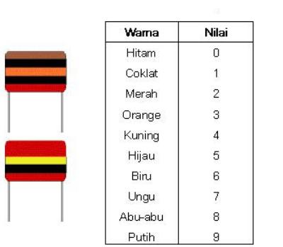
For polyester capacitor capacitance value can be identified by color as in the resistor.
The function of the use of capacitors in a circuit:

1. As the coupling between a single series with another series (in PS = Power Supply)

2. As a filter in the series of PS

3. As the generator frequency in the antenna circuit

4. To conserve power at the neon lights

5. Eliminate bounce (jump the fire) when installed on the switch

Capacitor Type

The capacitor consists of several types, depending on the dielectric material. For more simple can be divided into 3 parts, namely electrostatic capacitors, electrolytic and electrochemical.


Electrostatic Capacitor

Electrostatic capacitors are a group of capacitors that are made with a dielectric material of ceramic, film and mica. Ceramic and mica is a popular material and cheap to make small capacitance capacitors. Quantities available from pF to several μF, which is usually for a series of applications relating to high frequency. Groups including the dielectric film material is a material such as polyester (polyethylene terephthalate, or known as Mylar), polystyrene, polyprophylene, polycarbonate, metalized paper and others.

Mylar, MSM, MKT are some examples of the trademark name for the capacitor with a dielectric material film. Generally this group of capacitors is the non-polar.

Electrolytic Capacitors

Electrolytic capacitor group consisting of the capacitors dielectric materials are metal-oxide layer. Generally capacitor including this group is a polar capacitor with the + and - in the body. Why are these capacitors can have a polarity, is due to the manufacturing process uses electrolysis to form the positive pole and negative pole anode cathode.

It has long been known for some metals such as tantalum, aluminum, magnesium, titanium, niobium, zirconium and zinc (zinc) surface can be oxidized to form metal-oxide layer (oxide film). Oxidation layer is formed through a process of electrolysis, as in the process of gold plating. Metal electrode is dipped into the electrolyte solution (sodium borate) and given a positive voltage (anode) and the solution given electrolit negative voltage (cathode). Oxygen in electrolyte solution apart and oxidize the surface of the metal plate. For example, if used Aluminum, it will form a layer of aluminum-oxide (Al2O3) on the surface.


Thus successive metal plate (anode), layer-metal-oxide and the electrolyte (cathode) form a capacitor. In this layer-metal-oxide as the dielectric. From formula (2) great unknown capacitance is inversely proportional to dielectric thickness. Metal-oxide layer is very thin, and thus can be made ​​large enough capacitance capacitors.

Due to economical and practical reasons, generally a lot of metal material used is aluminum and tantalum. Materials are most numerous and cheap aluminum. To get a broad surface, Aluminum plate material is usually rolled radially. So in a way that can be obtained large capacitance capacitors. For example 100uF, 470uF, 4700uF and others, which often also called capacitor elco.

Electrolyte material in tantalum capacitors is a liquid, but there is also a solid. Called the solid electrolyte, but it is not the solution electrolit its negative electrode, but other materials are manganese-dioxide. Thus this type of capacitors can have large capacitance, but becoming more slender and petite. Also because of all the solid, then their work time (lifetime) to be more durable. Capacitors of this type also has a very small leakage current can be understood why so Tantalum capacitors become relatively expensive.


Electrochemical Capacitors

One other type of capacitor is an electrochemical capacitor. Including this type is a battery of capacitors and batteries. In fact, battery and capacitor batteries is very good, because it has a large capacitance and leakage current (leakage current) is very small. This type of capacitors of this type are also still in development to get a large capacitance, but small and light, for example for the application of electric cars and cellular phones.
READ MORE - Form and Type Capacitor